Deeply dig the cost of ASIC chip design, we asked the ProgPow core development team nine questions
Although ASIC chip design is not too advanced, it is not so easy to understand.
Overview
As long as it is related to the ProgPow and Ethash algorithms, there are various speculations on the hardware design and development cost of the mining machine, usually followed by an authoritative statement: please believe that the author of the prediction is because he/she is in the relevant industry. Has extensive experience in the field. These speculations are sometimes related to the production of cryptocurrency ASIC chips, and sometimes to integrated circuit design.
For those who are more familiar with the code but don't know much about fan-out and rise-times, this article may help them understand the ProgPow algorithm.
- Staking Economy (Series 6) predicts the challenges of future Staking economy and community ecology under the PoS consensus
- Most loved "dog coin" Musk
- Wall Street is always scared away? Are savvy investors ready, is the cryptocurrency ready?
(Eight Planet o-daily Note: Ethash is currently Ethereum's mining-based mining consensus algorithm, ProgPow is a mining algorithm that attempts to weaken the advantages of ASIC miners. Fanout is a digital signal that defines a single logic gate to drive. Enter the maximum amount of terminology. Most TTL logic gates can signal 10 other digital gates or drivers, so a typical TTL logic gate has 10 fanouts; rise time is a term used in pulse technology. The time interval between two voltage rises is the rise time of the network transformer.)
Programmers always give people a sense of omnipotence, from scripting to developing iPhone apps, from embedded systems to Windows operating systems. However, writing a code development application does not mean that you can become an authority on the APP Store app store backend (or improve system efficiency). Being able to develop a real-time multitasking operating system (RTOS) does not mean that you can become an extended Windows operating system. Weigh the people in the field.
Of course, as the core development team of ProgPow algorithm, IfDefElse does not mean that Windows designers are not "excellent programmers", but it must be explained that due to different technical backgrounds of different people, it is easy to cause understanding of different fields. Hypothesis is biased, especially when discussing economies of scale.
Similarly, a hardware designer may also be involved in different areas, such as designing a chip for an electric toothbrush or building a silicon architect for a network device. Engineers producing 100,000 electric home toothbrush chips may not understand the economies of scale that network engineers producing 1 million chips consider, and the same cryptocurrency ASIC chip designer may know little about GPU-ASIC chip design—these There is not much connection between the industries, and some even the gap between countries.
The last point we want to mention in the overview is that programming and engineering are actually a kind of skill. Unless you are programming code every day, you will soon fall behind and cannot become an authority, because the knowledge update iteration is very good. fast. Perhaps this is why it is difficult for new cryptocurrency ASIC manufacturers to enter the mining market based on the SHA-256 algorithm. After all, it is unlikely that a novice programmer wants to catch up with engineers who have studied the SHA-256 algorithm for six years.
On the other hand, there is not much article in the cryptocurrency ecosystem that introduces hardware knowledge. Of course, cryptocurrency itself is a software-led industry, and most hardware projects are “closed” in private companies.
Some "hardware bricks" are doing everything they can to ensure that software engineers can beat the cryptocurrency ecosystem – we have seen this in cryptocurrencies such as Monero, Bitcoin, and ZCash. appear. But the reality is that this challenge has not happened yet. Think about it. If Bitland or Innosilicon tries to make a CPU, do you think they can beat Intel and AMD?
Analyze ASIC chip design costs
Economies of scale are always ubiquitous – both in terms of cost and experience. For the cost of ASIC chip design, chip designers seem to have a lot of controversy. Let's take a look at the nine issues that are concerned about the industry: Let's take a look at the following issues:
Question 1: Regardless of whether the mining algorithm is ProgPow or ETHash, the hash value is determined by the storage bandwidth of the external dynamic random access memory (DRAM). Is this true?
But in fact, it's not. The hash of ProgPow is determined by two factors:
1, computing core
2, memory bandwidth
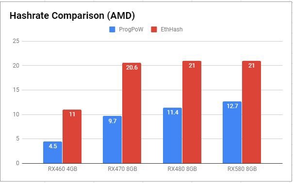
This is why there is a difference between Ethash and ProgPow, as shown in Figure 1 and Figure 2 below:
Figure 1: Comparison of mining hash rates for NVIDIA chip products
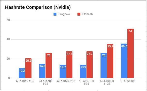
Figure 2: Comparison of mining hash rates for AMD chip products
At this stage, ETHash mining is more profitable, and the memory requirements for the algorithm are significantly increased. The growing demand for high-bandwidth memory has also led to the development of next-generation high-speed memory technologies such as GDDR6 (bandwidth speeds up to 768 GB/s). ) and HMB2 (bandwidth speed up to 256 GB/s).
Not all of the demand for high-bandwidth memory comes from “Ethash,” and the entire high-bandwidth memory market is worth $15 billion, with only a small percentage of it coming from the mining industry. The core market requirements for high-bandwidth memory include: GPUs, Field Programmable Gate Arrays (FPGAs), Artificial Intelligence (AI), High Performance Computing (HPC), and gaming. Compared to the $1.2 trillion artificial intelligence market, the $30 billion PC gaming market, the $35 billion handheld gaming market, and the $29 billion high-performance computing market, the high-bandwidth memory requirements of the mining industry are really "negligible".
Question 2: Since ProgPow's existing architecture and algorithms are similar to ETHash, will Innosilicon's next ASIC chip be tailored for ProgPow?
In fact, the only similarity between ProgPow and ETHash is the use of acyclic graphs (DAGs) in global memory. From a computational point of view, ETHash requires only a fixed "keccak_f1600" kernel and a modulo function. On the other hand, what ProgPow needs is a 16-channel wide random math sequence that also has access to the high-bandwidth L1 cache. Designing a computational kernel capable of executing ProgPow math sequences is much harder than designing a fixed function hash that can be similar to "keccak".
It's also important to note that the hash of ETHash depends only on the memory bandwidth, while the ProgPow algorithm depends on both the memory bandwidth and the core computation of the random math sequence—it's important to understand this.
The essence of the proof of work (PoW) is actually proved by the mathematical calculation of hardware and energy costs. As an algorithm, ETHash does not cost most of the hardware (calculation engine) in the mathematical proof. Instead, ETHash only captures the memory interface, which is why you can use an ASIC chip for cryptocurrency mining to eliminate uncaptured parts of the math.
Problem 3: Since the GPU is a general-purpose acceleration chip, the cycle of designing, manufacturing, and testing the GPU usually takes about twelve months, and a lot of hardware simulation and software development work is required to cover different computing scenarios and scenarios.
ProgPoW wants to capture the full hardware cost (as much as possible), since the updated part of the algorithm captures the computing hardware running different computing scenarios – up to the architectural wrinkles – so for ASIC chip designs, It takes more than 3-4 months.
Because of the long time span, another problem arises: Why is the floating point operation omitted? The answer to this question is actually very simple: floating-point operations cannot be ported across chips, and different chips tend to handle boundary cases related to special values (such as lower bounds, non-numeric values, and related variants) in different ways ( Corner case). A corner case is also referred to as a pathological case, a problem or situation in which the operating parameters are outside the normal range, and most of the cases are situations where several environmental variables or conditions are at extreme values, even if these extreme values are Also within the specification range (or boundary). The biggest difference is the handling of non-numeric values (NaN), which happens naturally when using random input, as explained in the Wikipedia page:
If there are multiple non-numeric (NaN) inputs, the payload result should come from one of the non-numeric values, but the standard does not specify.
This means that if you want to use floating-point arithmetic, basically every floating point needs to do "if(is_special(val))val = 0.0" check pairing, this check can usually be done in hardware, so it will also ASIC chips for cryptocurrency mining benefit from it.
Next, what is Hashrate and "hash-per-watt"?
Hash rate is a measure of energy costs. As long as everyone measures it in the same way, energy consumption per unit is less important – miners will continue to invest as much energy as possible. But even if you switch the unit of measure from 1 ETHash (smaller units, such as joules) to 1 ProgPow-hash (larger units, such as calories), the economics of operating costs will not change. Global Hashrate assesses the total economic weight of each person's protection of network sharing, as long as each person's contribution is fairly measured and uses the same unit. For ordinary miners, switching to the ProgPow algorithm does not take What changes come.
Of course, some would say that if Ethereum implemented the ProgPow algorithm, it might help concentrate the miners in large mines with high-end GPUs, and it would also spur the mine to upgrade the GPU to the latest models. But the ProgPow algorithm development team IfDefElse needs to reiterate that economies of scale will always exist, and it is also an unavoidable fact in the real world.
Problem 4: ASIC chip manufacturers can use smaller GDDR6 memory to get a cost advantage over GPUs. While maintaining the memory cost level, 16 GDDR6 4GB memory modules can achieve twice the bandwidth advantage, is this the case?
First, having twice the bandwidth advantage requires twice the computation. This is actually a linear scaling and cannot be seen as an advantage.
Second, we should not be ready for GDDR6 to produce 4GB memory chips. Micron (American Micron), the world's third-largest memory chip maker, only produces 8GB chips, while Samsung produces 8 GB and 16 GB chips. For memory chips, the GDDR6 IO interface area is very expensive, and each generation interface occupies more actual memory die than the memory cell, since the port physical layer (PHY) cannot pass through the process like a memory cell. The means are narrowed.
It is undeniable that some of the "long-cycle buyers", such as game consoles and GPUs, are really pushing the memory market. They also tend to support larger memory. In fact, today's memory vendors have no incentive to mass produce a 4GB of memory. After all, the market demand for this memory capacity is not large.
Problem 5: Many modules in the RTX2090 chip occupy a large number of chip die area, and are useless to ProgPow, including PCIE, NVLINK, L2Cache, 3072 slice unit, 64 ROP, 192 time measurement unit (TMU), etc. How to treat this problem?
The RTX2080 is not a good reference for discussing this issue. Due to some new features, some of Nvidia's RTX series chips occupy most of the chip's die area, such as the ray tracing core. The ProgPow design is paired with the stock chip products in NVIDIA and the AMD ecosystem, so new features in NVIDIA and AMD's new chip products cannot be used.
If you want a better analogy, perhaps the AMD RX 5xx series or the NVIDIA GTX 1xxx series is a good reference. As we mentioned earlier, some features in the GPU are not used by ProgPow, such as floating-point logic, secondary (L2) cache, and texture cache and ROP. The slice unit is where the vector math is executed, which is absolutely required by ProgPow. ASIC chips for cryptocurrency mining also want to add areas that enable "keccak" functionality. As a development team for the ProgPow algorithm, we estimate that the ProgPow ASIC chip's die area will be 30% smaller than the equivalent GPU – but even in the best case, its power consumption will only be reduced by up to 20%. In contrast, although some logic modules on the GPU are not fully utilized, resulting in wasted portion of the chip's die area, power consumption is minimal.
Question 6: Compared with large chips, will the revenue of small chips be higher?
How to say it is good, it sounds like it is popularizing chip manufacturing knowledge, maybe we need to write a training document for "Chip Manufacturing 101". In addition, for the income calculation formula, you can refer to a 2006 article " Comparative Logic-Array To ASIC-Chip Cost per Good Die ", in which you will find that chip revenue and process control are already large as early as 13 years ago. Innovative.
For a chip with a single functional unit, a chip with a smaller die area will have a higher yield than a chip with a larger die area. But for modern GPUs, this is not the case. Today's GPUs can be arbitrarily restored and combined, and the defects of small copy units are largely negligible. As long as each compressible functional unit is small enough, the GPU chip revenue can be as high as (or even higher) than a larger module with a functional module.
To better explain this concept, we can give a simple brain hole experiment:
1. Suppose you have a large chip "Giant ChipA" that occupies the entire chip. This "Giant ChipA" is made up of 100,000 detachable sub-assemblies, but it must be ensured that 80% of the sub-components are defect-free to ensure that "Giant ChipA" works properly. In the embedding process, the bad sub-components will Was bypassed.
2. Also, suppose you have a small chip "Tiny ChipB" that has only one functional module (not embeddable), but the small chip is small enough to fit 100,000 subassemblies on the same wafer. In this case, as long as one subcomponent is broken, it means that the entire "Tiny ChipB" chip is bad.
3. If there are 20,000 defective sub-components distributed evenly on each wafer, the “Giant ChipA” can earn 100% because they can remove 20% of defective sub-components, and “Tiny ChipB” The revenue may be only 80% because they cannot remove defective subcomponents.
If you look at AMD's Polaris 20 series and NVIDIA's GP 104 products, you'll find a large number of tiny "removable" submodules deployed in these GPUs under simulated lenses.
Problem 7: The ASIC miner voltage can be easily reduced to 0.4V, which is only one-half of the GPU… so the low-voltage ASIC design has been adopted by Bitcoin mining equipment ASIC miners, so now we don't have The reason is not to believe that they will not apply this strategy to the ProgPow ASIC mining machine. Can you talk about this?
Low-voltage design works when the chip is composed only of calculations, such as an ASIC miner specifically for the SHA256d mining algorithm. Integrating other artifacts—such as SRAM, which is required for ProgPow data caching—is extremely difficult and can't work at low voltages.
Question 8: The same energy-saving effect can also be achieved on LPDDR4x DRAM, and its power consumption is lower than GDDR6. Let's talk about this problem.
You can't just consider the power consumption problem. The bandwidth of LPDDR4x is much lower than GDDR6. The former has a bandwidth of 4.2Gb / s per pin and the latter is 16Gb / s. The LPDDR4x computing chip requires four times more memory chips and four times the memory interface to achieve the same performance as GDDR6, so the cost is actually significantly increased.
It is worth noting that the interface of high-bandwidth computing chips is usually limited, which means that the chip module area must be large enough that almost no signal is allowed to fall off the chip onto the printed circuit board (PCB). The LPDDR4x design needs to be approximately Four times the number of chip perimeter pads can reach the same bandwidth, that is, the cost is not only on the memory chip, but also the cost of the chip area is also calculated, so the overall cost is not low. . To make matters worse, since any chip is speed-oriented, when the chip module is larger, it means more wasted power.
So let's think about why today's GPUs can't run on LPDDR4x anymore. First, the performance of LPDDR4x in terms of bandwidth cost is not satisfactory. For a given bandwidth level (four times the number of chips), the cost of LPDDR4x is more than four times higher, which in turn leads to a significant increase in cost – LPDDR4x at 9W The cost of 256 GB/s bandwidth is about $150, compared to the same bandwidth cost of GDDR6 at 11W. The LPDDR4x doesn't save the miners any money. (Note, here is the bandwidth. Cost, not memory capacity cost).
Question 9: GPU makers like NVIDIA employ about 8,000 people to develop GPUs. These GPUs are also very complex; ASIC manufacturers like LinZhi employ only a dozen people and only develop ETHash mining algorithms. ASIC mining machine. The labor costs of these companies differ by 100, so it can be said that ASIC chips have an advantage over GPU chips in terms of cost and time to market.
What is to be said here is that economies of scale are an important factor. The GPU industry is also amortized in various sales channels around the world. The current total market size is approximately $420 billion, of which AMD has a market capitalization of approximately $11.6 billion, NVIDIA is approximately $154.5 billion, and the largest Intel is approximately $254.8 billion. In the memory market alone, the cost of physical ports (PHYs) and chips needs to be shared in an industry with a total size of $500 billion. The market value of Samsung Electronics with 320,671 employees is about $325.9 billion. They are also in the US. The most active patent applicant; the second is Micron Technology with 34,100 employees, with a market capitalization of approximately $60.1 billion, but the first chip manufacturer to develop 20Gbps high-speed GDDR6 memory; Hynix has 187,903 employees, market capitalization At around $56.8 billion, they developed the world's first 1Ynm 16Gb DDR5 DRAM. In contrast, the total market capitalization of the ASIC chip industry for cryptocurrency mining is only $146 billion, of which $73 billion is in bitcoin.
In addition, we have to look at the time-to-market and technology acceptance model (TAM), where we can refer to the development time of the famous S9 mining machine successor. If the fully-developed and computationally inefficient SHA256d algorithm compute chip takes three years to iterate, what can be done to ensure that the GPU-like ASIC miner supporting the ProgPow algorithm is quickly put into production? We can also analyze the recent ASIC mining machine mining Ethereum cryptocurrency. The GDDR6 chip sample trial period has been one year, and there is still no new version of the product that can be widely used.
The last thought of the ProgPow core development team IfDefElse
ProgPow is actually a mining hardware that is supported by economies of scale, has high visibility and gains a competitive advantage.
The ProgPow core development team IfDefElse is not large, and the team members also have full-time jobs, so they can't respond to all the questions and articles in time, and they don't have time to chatter in various cryptocurrency and blockchain forums. Although IfDefElse is very interested in hardware design and development, they still recommend that people involved in this field need to be cautious, because hardware and software are a diversified field, even if you are a cryptocurrency mining ASIC chip. Familiar big coffee, but may not be an expert in the GPU-ASIC field.
This article is from Medium, the original author is the ProgPow algorithm core development team IfDefElse
Translator: Odaily Planet Daily Translator | Moni
Source: Planet Daily
We will continue to update Blocking; if you have any questions or suggestions, please contact us!
Was this article helpful?
93 out of 132 found this helpful
Related articles
- From Wall Street veterans to bitcoiner, he believes privacy should be the default feature of Bitcoin
- How does the edge network relocate the data center?
- Payment giant PayPal first involved in the blockchain investment and participated in the Cambridge Blockchain A round of financing
- OKEx CEO Jay Open Letter: The decision to launch Jumpstart is really tough
- FCoin trading mining anniversary: the pass economy is not going to work
- Explore the ant blockchain Open Day: We have seen the arrival of the blockchain commercial era!
- Bitcoin skyrocketing is a bullish signal, or is it a return light?