In 2023, AI chip companies are undergoing a deadly three-question challenge.
AI chip companies face a critical three-question challenge in 2023.In 2023, investment institutions and shareholders launched a deadly three-question challenge to listed companies in the AI chip field:
Have you developed a storage and computation integrated chip?

(Investors questioning Lanqi Technology, image source: Tonghuashun Finance)
- In less than a week, MakerDAO has attracted a deposit of 700 million US dollars. Is the 8% interest rate really that enticing?
- Exploring the future trends of the NFT space through eths
- Even older than Ethereum itself? A Brief History and Current Situation of MEV
How is the progress of the storage and computation integrated chip?

(Investors questioning Dongxin Corporation, image source: Tonghuashun Finance)
What is the outlook for the storage and computation integrated chip?

(Investors questioning Hengshuo Corporation, image source: Tonghuashun Finance)
This series of questions indicates that the storage and computation integrated chip is no longer confined to academia and industry, but has become a hot topic in the secondary market. Shareholders and brokerage institutions are working overtime to catch up on storage and computation integrated chip knowledge. As a result, traditional chip manufacturers have been repeatedly questioned about their layout of the storage and computation integrated chip since the beginning of 2023.
A natural question arises: why has the storage and computation integrated chip suddenly become so popular?
Huawei, which released its new storage product OceanStor A310 on July 14, provides its own answer. Zhou Yuefeng, President of Huawei’s Data Storage Product Line, stated that there are many data challenges in training and reasoning for general and industry-scale models, such as slow cross-domain aggregation of massive data, low efficiency of data interaction in preprocessing and training, and difficulty in secure data flow.
AI large-scale models present new challenges to storage, such as lower stability compared to traditional AI models and a large amount of data preprocessing and preparation work. Near-storage computation (a form of storage and computation integration) is needed to systematically address this problem.
So, how much data is considered “a large amount”? According to estimates by Shrey Insight, the ChatGPT, which is currently active with 100 million daily users, would consume nearly a year’s worth of power generation from the Three Gorges Dam if 5% of people were to ask questions simultaneously every second.
In other words, large-scale models are demanding significant computing power, and emerging solutions like storage and computation integration can address many challenges posed by large-scale models. In fact, in addition to demanding high computing power, large-scale models have also provided AI chip manufacturers with “many opportunities”.
This article attempts to explore the benefits that AI chip manufacturers have gained under the background of large-scale models and the future prospects of storage and computation integrated chip manufacturers that have been “fueled” by ChatGPT.
LianGuaiRT-01: The “blessing and curse dependent” AI chip manufacturer
The wind of large-scale models is still raging, and discussions about them are still going on.
In early August, at the sub-forum “Jianjiangjian Kunlun: AI Large-scale Model Computing Power Frontier” of the Chinese Computer Society (CCF) Artificial Intelligence Conference, experts and scholars unanimously stated that in the era of large-scale models, intelligent computing power has become a “scarce asset.” How to make good use of computing resources and maximize their effectiveness has become a challenge that every participant must face.
Just GPT-3’s demand for computing power alone, in a conservative scenario, would require the Three Gorges Dam to work overnight to meet:
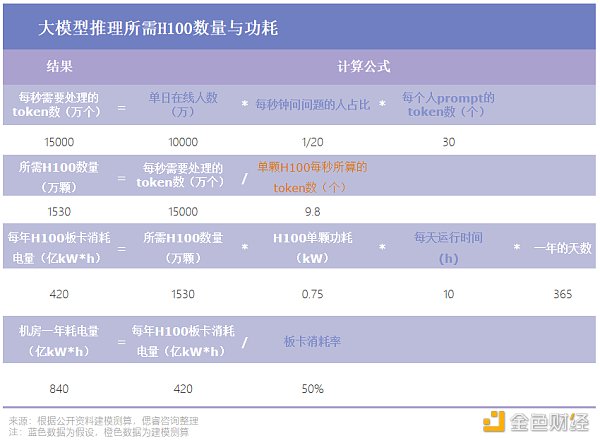
Assuming there are 100 million people online at the same time, with 5% of people asking questions every second, and each prompt taking up 30 tokens, it would require 15.3 million H100 chips to provide its reasoning power; and each H100 chip consumes around 750W of power, if running for 10 hours a day, the power consumption of the data center where these H100 chips are located will reach 84 billion kW*h per year, while the Three Gorges Dam generates 88.2 billion kW*h of electricity per year.
What makes AI chip manufacturers even more anxious is that this is only the power consumption of one big model, ChatGPT, during the reasoning stage. The power consumption of all the big models in all stages of operation is difficult to estimate.
Therefore, a series of emerging solutions have been explored by manufacturers: integrated storage and computing, chiplets, HBM, and so on. Among them, integrated storage and computing, which overturns the traditional von Neumann architecture’s storage wall, has truly achieved cost reduction and efficiency improvement, becoming this year’s “Polaris”.
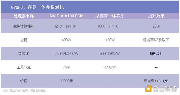
(Image source: Cai Rui Insight “AI Supercomputing Chip Industry Report – Innovators Take the Lead”)
In addition to the emergence of new solutions, which has given AI chip manufacturers a breather, big models have also brought good news to chip manufacturers, especially startups: the importance of software ecology is decreasing.
When the technology was not mature enough, researchers could only start with solving a specific problem, resulting in small models with parameter size less than one million. For example, DeepMind, an AI company owned by Google, had AlphaGo “learn” from millions of moves made by professional human players.
With the increase in the number of small models, hardware adaptation issues, such as chips, became urgent. Therefore, when Nvidia introduced the unified ecosystem CUDA, GPU+CUDA quickly gained recognition in the computer science community and became the standard configuration for artificial intelligence development.
Nowadays, emerging big models have multimodal capabilities, able to handle text, images, programming, and other problems, and can also cover multiple vertical fields such as office, education, and healthcare. This means that adapting to mainstream ecosystems is not the only option: when the demand for chips from big models soars, chip manufacturers may only need to adapt to 1-2 big models to complete orders that used to require multiple small models.
In other words, the emergence of ChatGPT provides an opportunity for startup chip manufacturers to overtake their competitors. This means that the AI chip market landscape will undergo a huge change: it will no longer be a monopoly of individual manufacturers, but a collective effort of multiple innovators.
When computing power becomes scarce, and adapting to mainstream ecosystems is no longer a prerequisite, integrated storage and computing cannot hide its brilliance. At this time, the second difficult question facing AI chip manufacturers is whether or not to invest, and how much to invest.
Regarding this, the answer given by “veteran” chip giant NVIDIA, who has been struggling for many years, is to be innovative and invest heavily:
Every emerging technology manufacturer undoubtedly faces technical exploration obstacles in the early stages, as well as various issues such as downstream manufacturers not recognizing it. In the early stages, whoever first predicts the future development trend and dares to take exploratory steps and lays down reasonable resources to try it out will seize the opportunity.
When the wave of data centers had not yet swept the world and artificial intelligence training was still a niche field, NVIDIA had already invested heavily in the research and development of general-purpose computing GPUs and the unified programming software CUDA, in order to secure a good job for NVIDIA – a computing platform.
At that time, making GPUs programmable was “useless and unprofitable”: it was unknown whether their performance could double, but the product development would double. As a result, no customers were willing to pay for it. However, NVIDIA, who foresaw that a single-function graphics processor was not a long-term solution, decisively decided to apply CUDA to all product lines.
In an interview with Dr. Lai Junjie, director of engineering and solutions for NVIDIA China, he said, “In order to achieve the vision of a computing platform, Huang Renxun quickly mobilized a lot of resources from top to bottom in NVIDIA in the early stages.”
Vision + heavy investment, in 2012, NVIDIA received the reward of an innovator: in 2012, the computational performance of deep learning algorithms caused a sensation in the academic community. As a high-performance and more versatile and user-friendly productivity tool, GPU+CUDA quickly became popular in the computer science world and became a “standard configuration” for artificial intelligence development.
In the journey of AI’s high-performance computing chips, the era of storage and computing integrated chips has come to its “golden period”, and forward-looking investment is the correct answer.
LianGuaiRT-02 Those without technical expertise and abundant resources, please stay away
Seeing the various benefits of storage and computing integration, the camp of players in the storage and computing integrated chip field is growing.
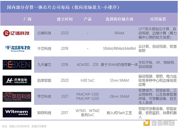
(Image source: Cai Rui Insight “AI High-Performance Computing Chip Industry Report – A Hundred Boats Competing, Innovators First”)
According to incomplete statistics from Cai Rui Insight, since 2019, most of the new AI chip manufacturers have been focusing on storage and computing integration: there have been 20 new AI chip manufacturers from 2019 to 2021, among which 10 have chosen the storage and computing integrated route.
This indicates that storage and computing integration will become a rising star after architectures such as GPGPU and ASIC. However, not everyone can grasp this rising star.
In the academia, industry, and capital markets, storage and computing integration is unanimously favored. Strong technical capabilities, solid talent reserves, and precise control over the acceptance of migration costs are key to maintaining competitiveness for startups in the industry and the three major barriers in front of new players.
Strong technical strength is always the highest peak in the field of chips.
First of all, it has a wide range of “involvement” in storage and calculation integration, involving every aspect of chip manufacturing: from the bottom-level devices to circuit design, architecture design, toolchain, and software development. Secondly, it “affects the whole body with a slight move”: while making corresponding changes at each level, it also needs to consider the adaptability between different levels.
Let’s take a look at the technical challenges of creating a storage and calculation integrated chip layer by layer.
Firstly, in terms of device selection, manufacturers have to be “extremely cautious”: the design of memory determines the yield of the chip, and once the direction is wrong, the chip may not be mass-produced.
Secondly, at the circuit design level, after having the devices, it is necessary to design the circuit for storage arrays. Currently, there is no EDA tool guidance for circuit design in storage and calculation, so it needs to be done manually, which undoubtedly increases the difficulty of operation.
Next, at the architectural level, after having the circuit, it is necessary to design the architecture. Each circuit is a basic computing module, and the design of the storage and calculation integrated module determines the energy efficiency of the chip. Analog circuits will be affected by noise interference, and the chip will encounter many problems when affected by noise.
In this case, chip architects need to have a sufficient understanding of the process characteristics of analog storage and calculation, and design the architecture based on these characteristics. On this basis, they also need to consider the adaptability between architecture and software development. After the architectural design at the software level is completed, the corresponding toolchain needs to be developed.
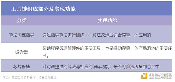
(Image Source: Cai Rui Insight “AI High Computing Power Chip Industry Report – Innovators First”)
Due to the difference between the integrated storage and calculation model and the traditional architecture model, the compiler needs to adapt to a completely different storage and calculation integrated architecture to ensure that all computing units can be mapped to the hardware and run smoothly.
After going through a complete technical chain, it tests the capabilities of the device, circuit design, architecture design, toolchain, and software layer development, as well as the coordination and adaptability of each link. It is a time-consuming, laborious, and costly endurance battle.
At the same time, according to the above process flow, it can be seen that companies that can achieve storage and calculation integration urgently need experienced circuit designers and chip architects.
Considering the uniqueness of storage and calculation integration, companies that can achieve storage and calculation integration need to have the following two characteristics in terms of personnel reserves:
1. The leader needs to have enough courage. They should have a clear idea in the selection of devices (RRAM, SRAM, etc.) and calculation modes (traditional von Neumann, storage and calculation integration, etc.). This is because storage and calculation integration is a subversive and innovative technology, and without a leader, the cost of trial and error is extremely high. Enterprises that can achieve commercialization often have founders with rich industry experience, experience in large factories, and academic backgrounds, who can lead the team to quickly complete product iterations.
2. In the core team, experienced talent is required at various levels of technology. For example, the architect is the core of the team. The architect needs to have a deep understanding and cognition of the underlying hardware and software tools, and be able to implement the conceptual storage and computing architecture through technology to ultimately achieve product implementation;
3. In addition, according to a report from Quantum Bit, there is a lack of high-end talent in circuit design in China, especially in the field of mixed circuits. Storage and computing involve a large number of analog circuit designs. Compared with digital circuit designs that emphasize team collaboration, analog circuit designs require individual designers who are extremely familiar with process, design, layout, model PDK, and packaging.
And this series of talent and technology should all be aimed at the ultimate goal of implementation – implementation is the primary productivity. When delivering, customers consider not only the storage and computing integrated technology, but also whether the overall SoC energy efficiency ratio, area efficiency ratio, usability and other performance indicators of the storage and computing integrated technology have been sufficiently improved compared to previous products. More importantly, is the migration cost within the acceptable range.
If choosing a new chip to improve algorithm performance requires learning a new programming system, and the labor cost of model migration is higher than the cost of buying a new GPU, then customers are unlikely to choose to use the new chip.
Therefore, whether the storage and computing integrated technology can minimize migration costs during the implementation process is a key factor for customers when choosing a product.
In the context of large models, storage and computing integrated chips, with their characteristics of low power consumption but high energy efficiency ratio, are becoming a rising star in the chip race. Nowadays, the storage and computing integrated market is still in a stage of “just showing its potential”.
But what we cannot deny is that storage and computing integrated players have already built three strong barriers, and those without strong technical strength and solid talent reserves should not enter.
We will continue to update Blocking; if you have any questions or suggestions, please contact us!
Was this article helpful?
93 out of 132 found this helpful
Related articles
- Function hidden in the LianGuaiyLianGuail stablecoin code can freeze assets and clear addresses.
- LD Capital Understanding the Current Situation of CyberConnect in One Article
- Web3 advertising startup HypeLab has completed a $4 million financing round, led by Shima Capital and Makers Fund.
- Onchain Summer has started. How to play with the Base chain?
- LianGuaiWeb3.0 Daily | Hong Kong-listed companies have approved a budget of $5 million to purchase cryptocurrencies.
- Grasp the opportunity of MEKE public beta and seize the core of Binance Chain Odyssey.
- Analyzing the Landscape of Investment DAOs Definitions, Categories, Structures, and Design Space


